The bulk of my undergraduate laboratory life at Cornell was spent in the Bazarov lab, working with Luca Cultrera and a multitude of collaborators on a variety of projects, as well as being a general wrench monkey when necessary.
A variety of applications, ranging from accelerator physics to certain medical scans, require a highly collimated electron beam. These beams are produced via the photoelectric effect, by shining a light on a semiconductor surface which releases electrons. The materials studied in our lab were mainly alkali antimonides and related compounds, e.g. Na2KSb, Cs3Sb, and Cs2Te. These are semiconductors which emit electrons when illuminated with light in the visible spectrum. Alkali antimonides are unstable in the presence of air and water, and so must be grown, stored, and analyzed under ultra high vacuum (UHV), generally at or below 10-10 Torr.
A good photocathode has a two important qualities: high quantum efficiency and low mean transverse energy. The quantum efficiency (QE) is a measure of how many photons are needed to excite an electron. The mean transverse energy (MTE) is a measure of the momentum spread of the electron beam, a quantity which is corrected for with bunchers and solenoids in the beamline but is important to get right at the material level. In general, it's difficult to simultaneously minimize MTE and maximize QE at visible wavelengths, so typically MTE would take precedence.
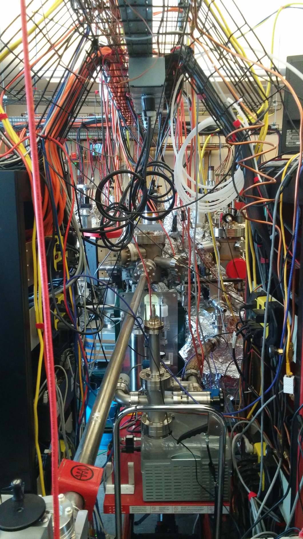
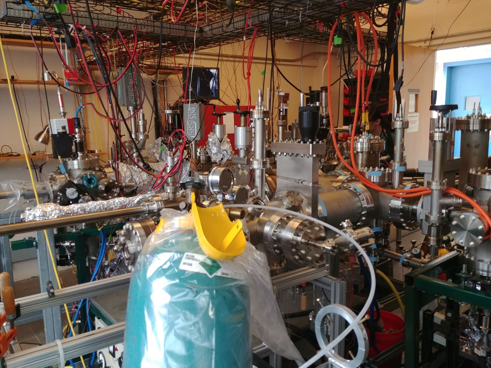
Our lab occupied roughly half of Newman Laboratory (including an office, according to Peter Lepage, where Ken Wilson came up with his theory of renormalization!). Some of our facilities included two growth chambers utilizing chemical vapor deposition (CVD), an Auger spectrometer, a Mott polarimeter, and a custom-made setup for measuring MTE (termed the TEMeter, pronounced "tee-ee-meter"). Future installments will include a cryogenically cooled TEMeter and a beamline with a 50 Watt (!) laser as a tunable IR to UV light source. The main growth and analysis chamber, pictured to the right in all its wiry glory, was termed the Mother chamber. Of course, photocathodes in an accelerator lab are no good if they can't be put into an accelerator, so a vacuum "suitcase" was used to transport samples from Newman lab to the beamline at CHESS in Wilson lab.
Part of the day-to-day maintenance of a UHV chamber involves "baking" after opening. The two worst enemies of vacuum are oil and water. Oils, like those secreted from your fingertips, are difficult to remove without doing a deep cleanse with soap and alcohol, but they're not a problem with proper hygeine and use of nitrile or latex gloves. Water, on the other hand, immediately adsorbs to the metal surface upon contact with air and will outgas constantly if it's not taken care of. After a chamber is opened, it's sealed shut, wrapped in heat tape and a few layers of heavy duty tin foil (for heat distribution and insulation), and heated to around 150°C for a couple of days to vaporize any adsorbed water. Baking is the gruntiest of grunt work; you'll get cuts on your hands from the tin foil, bumps on your head from crawling under the chamber, and you'll struggle to avoid burning out improperly wrapped heat tapes. I enjoyed it immensely.
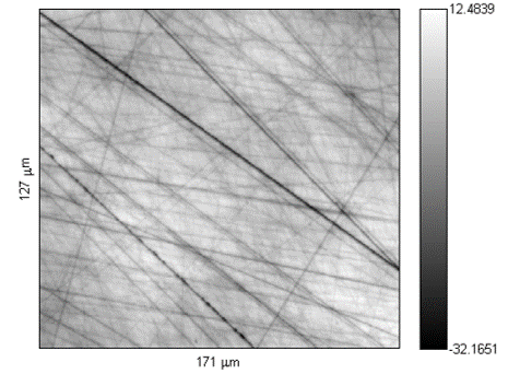
One tool lacking from that list of devices is something to measure surface roughness, a vitally important element in creating a high brightness beam. Rough photocathodes mean high MTE at the surface, and thus an imperfect beam profile. It was therefore important to come up with a technique to noninvasively measure the roughness of the photocathodes. Due to a formula by Davies [1], and as summarized by Bennett and Porteus [2], there is a precise relationship between RMS roughness \( \sigma \) and surface reflectivity given by $$\sigma = \frac{\lambda}{4 \pi \cos \theta} \sqrt{ - \ln \left( \frac{R}{R_0} \right)}$$ for wavelength \( \lambda \), angle of incidence \( \theta \), total reflectance \( R_0 \), and specular reflectance \( R \). With this relation, we were able to verify measurements of surface roughness taken with a profilometer with only a few lenses and a power meter.
While optical methods may have sufficed to get an estimate of surface roughness, nothing beats a real measurement. Through a collaboration with Melissa Hines in the chemistry department, we got access to a scanning tunneling microscope (STM) in Baker Lab, which was inconveniently a parking lot away from Newman Labs where the cathodes were grown. To add to the complications, under normal operating circumstances, the STM would be opened under atmosphere, the sample would be inserted, and the system would be pumped down, a procedure which would compromise our photocathodes. We therefore had to design a vacuum "suitcase" to transport cathodes under UHV from Newman Lab to Baker Lab, along with a manipulator and gate valve system to get the sample inside under vacuum. It took a while to get the system working, due to a few unfortunate gate valve failures and difficult in creating a proper manipulator inside the vacuum, but we were eventually able to transfer and scan a sample of bright baby blue cesium telluride with the STM.
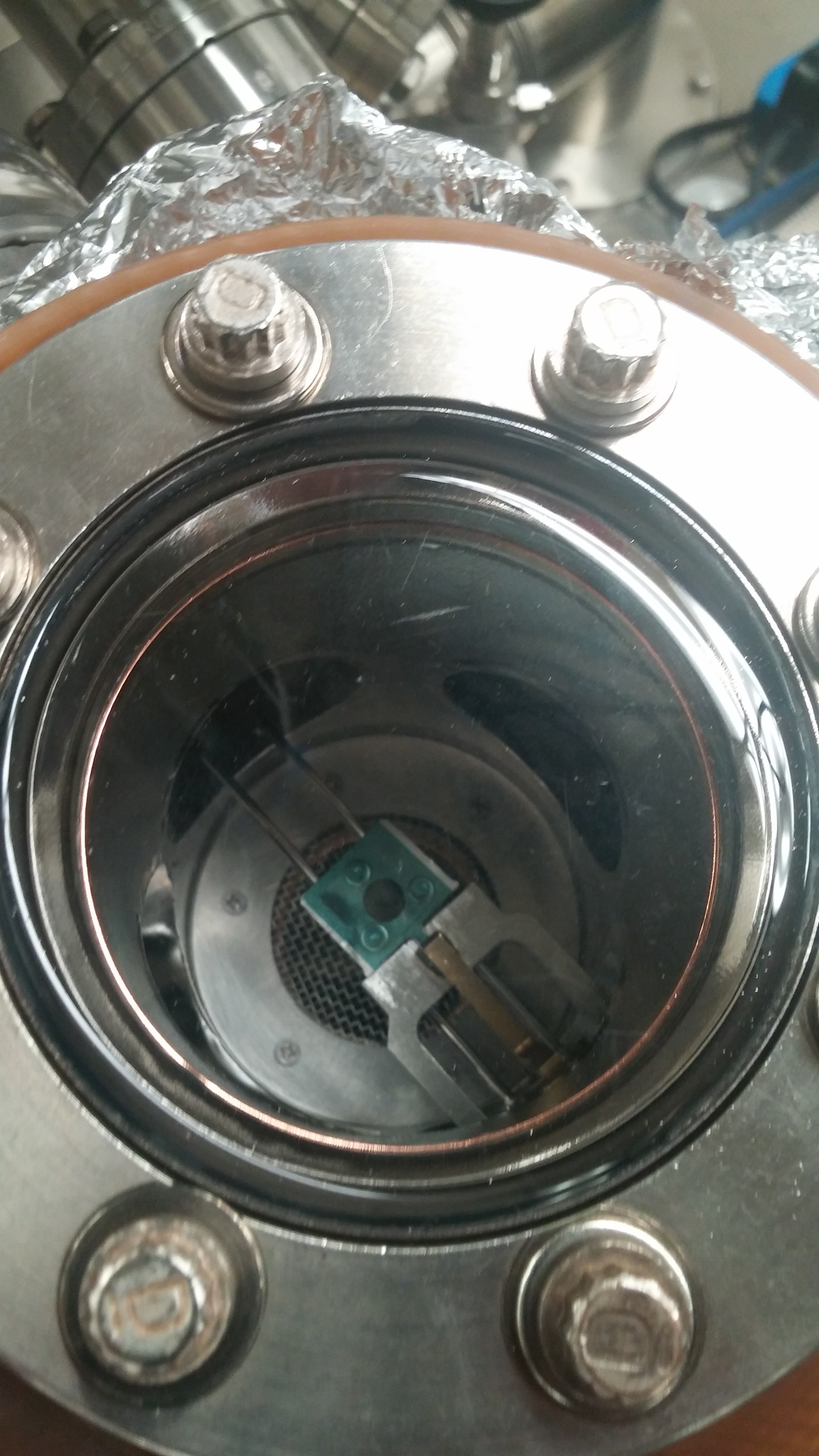
The transfer system underwent a great deal of evolution in the 3-4 years of its construction. As part of the NSF-funded Center for Bright Beams (CBB), we also began collaborating with Kyle Shen, designing a universal sample holder that would allow us to take measurements with both STM and angle-resolved photoelectron spectroscopy (ARPES). This sample holder was based on the standard sample holder for the Omicron STM, but with an elevated platform for ARPES measurements. Prototypes were constructed out from stainless steel, but the final product was made of paramagnetic niobium. Eventually, this sample holder may be used to conduct experiments at other facilities such as Brookhaven National Lab, as well as for further collaboration with molecular beam epitaxy (MBE) fabrication groups at Cornell.
[1] H. Davies, "The Reflection of Electromagnetic Waves From a Rough Surface," Proceedings of the IEE - Part IV: Institution Monographs 101 no. 7, (August, 1954) 209-214. [2] H. E. Bennett and J. O. Porteus, "Relation Between Surface Roughness and Specular Reflectance at Normal Incidence," J. Opt. Soc. Am. 51 no. 2, (Feb, 1961) 123-129.