The revolutionary photon-counting detector technology at the core of Mazin Lab research
Cryogenic Detectors for Astronomy, Bio-Imaging, and Quantum Information
Cryogenic detectors, with operating temperatures on the order of ~100 mK, are currently the preferred technology for astronomical observations over most of the electromagnetic spectrum, notably in the far infrared through millimeter (0.1–3 mm), X-ray, and gamma-ray wavelength ranges. In the important ultraviolet, optical, and near infrared (0.1–5 µm) wavelength range, a variety of detector technologies based on semiconductors — backed by large investment from both consumer and military customers — has resulted in detectors for astronomy with large formats, high quantum efficiency, and low readout noise. However, these detectors are fundamentally limited by the band gap of the semiconductor (1.1 eV for silicon) and thermal noise sources from their relatively high (~100 K) operating temperatures.
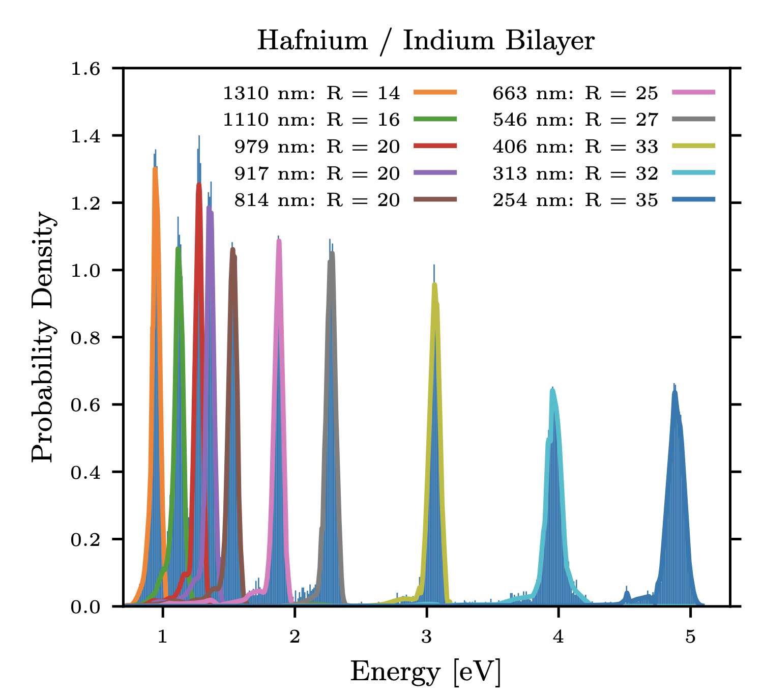
Cryogenic detectors allow the use of superconductors with gap parameters roughly 10,000 times lower than semiconductors. This difference allows a leap in capabilities. A superconducting detector can count single photons with no false counts while determining the energy (to several percent or better) and arrival time (to a microsecond) of the photon. This is the optical analog of an X-ray microcalorimeter. It can also have much broader wavelength coverage since the photon energy is always much greater than the gap energy. While a CCD is limited to about 0.3–1 µm, the MKIDs described here are in principle sensitive from 0.1 µm in the UV to greater than 5 µm in the mid-IR, enabling observations at infrared wavelengths vital to understanding exoplanets.
Microwave Kinetic Inductance Detectors (MKIDs)
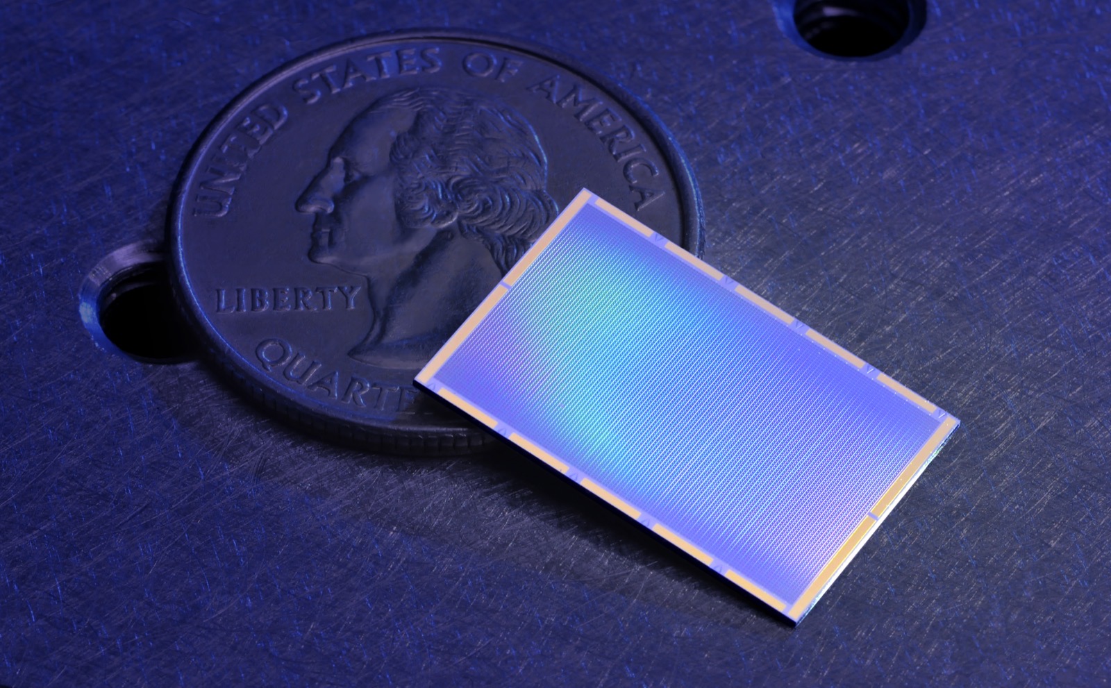
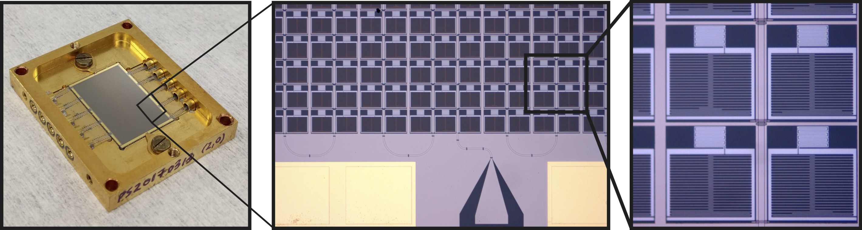
Microwave Kinetic Inductance Detectors, or MKIDs, are a cryogenic detector technology that has proven important for astrophysics due to their sensitivity and the ease with which they can be multiplexed into large arrays. MKIDs use frequency domain multiplexing that allows thousands of pixels to be read out over a single microwave cable. The Optical Lumped Element (OLE) MKID arrays developed by the Mazin Lab have significant advantages over semiconductor detectors like charge coupled devices (CCDs). They can count individual photons with no false counts and determine the energy and arrival time of every photon with good quantum efficiency. Their physical pixel size and maximum count rate are well matched with large telescopes. These capabilities enable powerful new astrophysical instruments usable from the ground and space.
How MKIDs Work
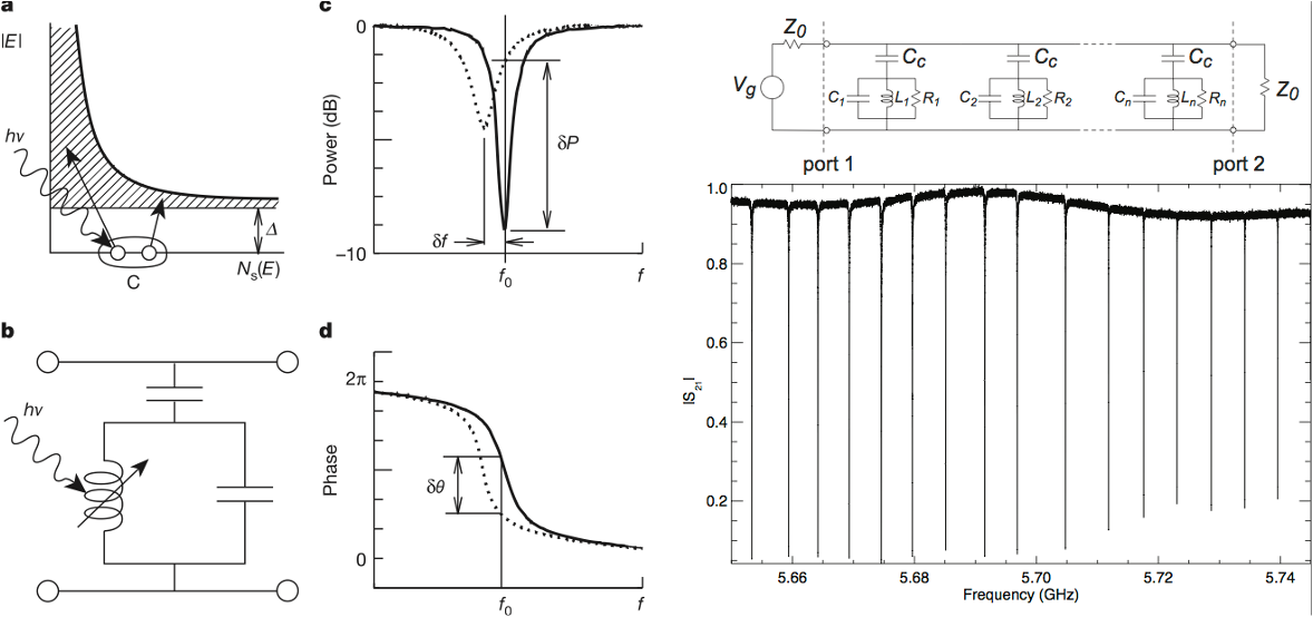
MKIDs work on the principle that incident photons change the surface impedance of a superconductor through the kinetic inductance effect. The kinetic inductance effect occurs because energy can be stored in the supercurrent of a superconductor. Reversing the direction of the supercurrent requires extracting the kinetic energy stored in the supercurrent, which yields an extra inductance. This change can be accurately measured by placing this superconducting inductor in a lithographed resonator.
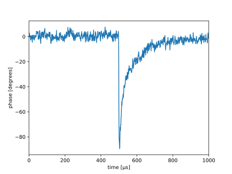
A microwave probe signal is tuned to the resonant frequency of the resonator, and any photons absorbed in the inductor will imprint their signature as changes in phase and amplitude of the probe signal. Since the quality factor Q of the resonators is high and their microwave transmission off resonance is nearly perfect, multiplexing can be accomplished by tuning each pixel to a different resonant frequency with lithography during device fabrication. A comb of probe signals can be sent into the device, and room temperature electronics can recover the changes in amplitude and phase without significant cross talk.
Key References
- A broadband superconducting detector suitable for use in large arrays. Day et al., Nature, 2003.
- Position sensitive x-ray spectrophotometer using microwave kinetic inductance detectors. Mazin et al., Applied Physics Letters, 2006.
- Experimental evidence for a surface distribution of two-level systems in superconducting lithographed microwave resonators. Gao et al., Applied Physics Letters, 2008.
- A superconducting focal plane array for ultraviolet, optical, and near-infrared astrophysics. Mazin et al., Optics Express, 2012.
- A readout for large arrays of microwave kinetic inductance detectors. McHugh et al., Review of Scientific Instruments, 2012.
- Superconducting Microresonators: Physics and Applications. Zmuidzinas, Annual Review of Condensed Matter Physics, 2012.
- Development of Microwave Kinetic Inductance Detectors for Applications in Optical to Near-IR Astronomy. Szypryt, Ph.D. Thesis, UCSB, 2017.