")
A diode, also known as a rectifier, is a device that passes current in one direction, but not in the opposite direction. Such a device has many important uses, perhaps the most obvious one being to change AC into DC (see demonstrations 64.57 -- Half-wave rectifier, 64.58 -- Full-wave rectifier and 64.59 -- Bridge rectifier). Early rectifiers were vacuum tube devices, in which a voltage applied in one direction drove electrons emitted from a heated cathode to the anode, thus producing a current. If the potential were reversed, the electrons would be repelled back toward the cathode, and no current could flow. Current could flow only when the potential on the anode was positive with respect to that on the cathode. The vast majority of rectifiers are now semiconductor devices.
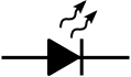
The schematic symbol for a diode is:
As the symbols are oriented above, the wire on the left goes to the anode, and the wire on the right goes to the cathode. Most diodes have a band to denote the cathode end. Most LEDs that have a round case, as the one shown in the photograph above, have a longer lead on the anode than on the cathode, and a flat near the cathode lead.
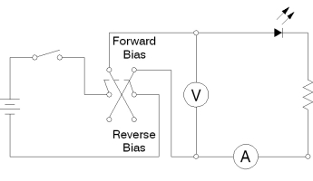
This demonstration allows you to apply a potential across an LED and a series current-limiting resistor in either direction, and to display the potential and the resulting current through the LED (though not at the same time). It is wired according to the following schematic:
Selecting “DCV” on the multimeter displays the voltage across the LED/resistor combination, with its direction indicated by the absence or presence of a minus sign, and selecting “DC mA” displays the current through the LED/resistor combination. (The milliameter input completes the circuit no matter which setting you choose, so switching between settings does not interfere with the operation of the circuit.)
With the LED forward biased, the current is approximately 15 mA, and the LED glows, as shown in the photograph above. In this case, switching to the voltmeter gives a reading of approximately +3 V. When you flip the DPDT switch to “Reverse Bias,” the voltage reading changes to approximately -3 V, the current drops to 0 mA, and the LED is no longer lit.
One could, of course, perform this demonstration with a regular diode, showing the current in forward and reverse bias conditions. The light emitted from the LED when it is forward biased, though, gives an additional visual cue to what is happening.
How does it work?
Materials are often broadly classified as conductors or insulators. For a substance to be a conductor, its electronic structure must be such that there are unoccupied energy levels close enough in energy to where the valence electrons normally reside that the electrons can easily be excited to those levels. In doing so, they leave vacancies (holes), which may then be filled by other electrons, thus allowing the electrons to move about the crystal lattice of the material, and a current to flow. These energy levels comprise what is commonly called the conduction band. The levels occupied by the unexcited valence electrons are known as the valence band. In an insulator, the conduction band lies at sufficiently high energy above the valence band that the valence electrons cannot easily reach the levels that lie there, and the material does not conduct electricity. This energy difference is called a band gap. In some materials, the band gap is much smaller than that of an insulator, and the electrical conductivity is intermediate between that of a conductor and that of an insulator. Such materials are called semiconductors.
With the exception of hydrogen, all elements lying to the left of group 13 (IIIa, headed by boron) are metals, and thus good conductors. Those lying to the right of a stepped line going roughly from boron to astatine are nonmetals, and thus insulators. Those elements lying between the groups of metals and nonmetals are semimetals. The most commonly used elements in semiconductor devices are probably silicon and germanium. One can increase the electrical conductivity of a semiconductor by doping it with a small amount of certain other elements that have either one more or one fewer valence electron than does the semiconductor in question. For example, silicon, which is in qroup IVa, has four valence electrons, each of which participates in a bond in the crystal lattice. If an arsenic atom, which has five valence electrons, replaces a silicon atom, it then has one electron left over, which cannot participate in bonding and is thus available for conduction. Thus, doping silicon with a small amount of arsenic produces an n-type semiconductor. If, instead, one substitutes some boron atoms, which have only three valence electrons, this results in electron vacancies in the crystal lattice, or holes. When an electron moves to fill one of these holes, it leaves behind another hole. This type of semiconductor is called p-type. Thus, we speak of the charge carriers in n-type material as being electrons, and in p-type material as being holes. There are, of course, other combinations of elements one can use to make these types of semiconductors. In addition, there are now organic semiconductors and conductors. One of the pioneers in the development of these materials is the UCSB physics department’s own Prof. Alan Heeger, who, with Alan G. MacDiarmid and Hideki Shirakawa, was awarded the Nobel Prize in Chemistry in 2000 for this work.
The simplest semiconductor device is a p-n junction. That is, a piece of p-type material and a piece of n-type material placed in contact with each other. If no external potential is applied, some of the electrons in the n-type material can cross the junction to fill holes in the p-type material. This leaves a positive charge on the n-type section and a negative charge on the p-type section, which prevents further flow of charge carriers across the junction. The resulting potential is called the contact potential or junction potential. We will see that we must overcome this junction potential in order to make the diode conduct electricity.
If we reverse bias the junction, that is, place a potential across it so that the n-type section is positive with respect to the p-type section, any electrons in the p-type region cross back over the junction into the n-type region, where all the electrons are drawn away from the junction toward the positive supply terminal. Similarly, any holes that were in the n-type region are filled, and the holes in the p-type region are drawn toward the negative terminal. The junction is thus depleted of charge carriers, and current cannot flow.
If we bias the junction in the forward direction, that is, put a potential across it so that the p-type section is now positive with respect to the n-type section, the electrons in the n-type material are repelled from the negative power supply terminal, as are the holes in the p-type region repelled from the positive terminal. The electrons in the n-type region are drawn toward the junction, which they can now cross to fill the holes in the p-type region, leaving more holes behind in the n-type region. Current can now flow, and the diode conducts. Since the aforementioned junction potential is opposite to the forward bias potential, whatever potential we apply must exceed this junction potential in order for the diode to conduct. The cathode is the n-type region, and the anode is the p-type region.
In the LED, the current that flows with forward bias is accompanied by the emission of light. When an electron crosses the p-n junction, it can relax from either a level in the conduction band or a donor impurity level to either an acceptor impurity level or a level in the valence band. This gives rise to emission of light over a narrow band of wavelengths. If one chooses the proper materials and dopants, one can tune the size of the band gap so that energy of the emitted light falls in the desired range of the spectrum, from near IR, through the visible range, to near UV. The first such diodes were of the gallium-arsenide-phosphide type, and they emitted in the infrared at about 900 nm.
References:
1) David Halliday and Robert Resnick. Physics, Part Two, Third Edition (New York: John Wiley and Sons, Inc., 1978), p. 567.
2) Steven S. Zumdahl. Chemical Principles, Third Edition (Boston: Houghton-Mifflin, 1998), pp. 553-4, 754-7.
3) Howard V. Malmstadt, Christie G. Enke and Stanley R. Crouch. Electronics and Instrumentation for Scientists (Menlo Park, California: The Benjamin/Cummings Publishing Company, Inc., 1981), pp.53-56.
4) A. James Diefenderfer. Principles of Electronic Instrumentation, Second Edition (Philadelphia: W.B. Saunders Company, 1979), pp. 410-11.
5) For a comprehensive overview of the theory of conduction in solids, which finishes with a section on semiconductor devices, see chapter 13 of Quantum Physics of Atoms, Molecules, Solids, Nuclei and Particles by Robert Eisberg (A UCSB professor emeritus!) and Robert Resnick (New York: John Wiley and Sons, 1974), pp.483-521, “Solids – Conductors and Semiconductors.”