The text for demonstration 64.56 -- Light-emitting diode (LED), gives an explanation of how a diode works. The diode comprises a single p-n junction, and it allows current flow in only one direction. The next step in complexity is to add a third semiconductor layer to form a (bipolar) transistor. The development of the transistor came when, sometime around the early 1940s, AT&T, hoping to expand their telephone system, was seeking a replacement for the vacuum tubes then used to amplify signals. Vacuum tubes were large, generated large amounts of heat and drew too much power to be used in great numbers. In addition, they were too slow, and not capable of the frequency response that AT&T desired. To develop an amplifier based on a semiconductor device, AT&T had Bell Laboratories, their research division, assemble a team under the leadership of William Shockley. Among those he recruited for the effort were John Bardeen and Walter Brattain. Their efforts led to the development of the first transistor, for which they were recognized with the 1956 Nobel Prize in physics. You can find a summary of the events, with references, at this link. Shockley, Bardeen and Brattain called their device a “point contact” transistor. It was a type of transistor known as a field effect transistor. In this type of transistor, current flow through a semiconductor is controlled by means of a “gate” made of a piece of opposite-polarity semiconductor, placed in the middle of the first. By biasing this gate appropriately with respect to one end of the other piece of semiconductor, one can vary the degree of charge depletion at the junction with the gate, and thus control current flow through the device. The transistor in this demonstration is not of this type, but, rather, is a bipolar transistor. In addition, since it is made to carry large currents and operate at fairly high voltages, it is also a power transistor.
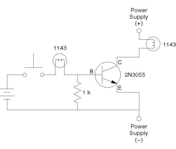
A bipolar transistor is a three-layer device, comprising either a thin layer of p-type material sandwiched between two layers of n-type material (npn), or a thin layer of n-type material sandwiched between two layers of p-type material (pnp). Going from one end to the other, these are called, respectively, the collector, base and emitter. The electronic schematic symbol for an npn transistor is the symbol next to the number “2N3055” in the schematic below, with the letters “C,” “B” and “E,” for “collector,” “base” and “emitter.” 2N3055 is the type of npn power transistor in this demonstration. The symbol for a pnp transistor is similar to the one below, except that the arrow of the emitter points in toward the base. A convenient mnemonic to remember which symbol stands for which type of transistor is to let “npn” stand for “not pointing in.” The two junctions in this device act individually as diodes, as you might expect. In fact, in most cases, a good way of testing a bipolar transistor is to take an ohmmeter and alternately bias the base-emitter junction in both directions and the base-collector junction in both directions. For example, in an npn transistor, you should get continuity when the base is positive with respect to either the emitter or the collector, but not when it is negative with respect to them. For either junction (as for a diode), infinite or exceedingly high resistance in the forward bias direction indicates an open junction, and low resistance in the reverse bias direction indicates a shorted junction. (Of course, if the transistor is still in circuit, such a test may not be possible, depending on the circuit.)
Normally, as in the schematic below, the collector-base junction is reverse biased, and the base-emitter junction is forward biased. Here, the collector is connected through the light bulb (1143 – 12.5 V, 1.98 A) to the positive side of a power supply, and the emitter is connected to the negative terminal of the power supply. With the pushbutton switch open, no current can flow, since the reverse-biased collector-base junction has a very high resistance. The 1-k resistor between the base and the emitter is just to make sure that as long as the switch is open, the base remains at ground potential. Pressing the button connects the positive terminal of the battery to the base via a second light bulb, thus raising its potential relative to that of the emitter, which is tied to the negative terminal of the battery, and thus forward biasing the base-emitter junction. Current now flows from the base to the emitter. Since the base region is thin and lightly doped, electrons entering from the emitter are attracted to the collector because of the potential difference between it and the base. Current thus flows from the collector through to the emitter, lighting the light bulb (connected to the collector).
To show how the bulb looks when it is connected directly across the power supply, you can touch the free end of the black jumper to the outside of the lamp socket, or to the bracket that holds it. Then when you press the button to turn the transistor on, the class can see that the bulb glows just as brightly as if it were connected directly to the supply.
The base current (approximately 700 mA in this particular circuit) is much smaller than the collector current (about 2 A in this circuit). The voltage applied to the base (which ends up at about 0.9 V) is also much smaller than the change in voltage difference between the collector and emitter, which goes from 12 V (actually significantly higher, because the unloaded power supply sits at about 16 V) to about 0.15 V. This amplification phenomenon, whereby one can control a large current with a small current, or where a small change in voltage on the input of the circuit gives rise to a large change in voltage on the output, is called the transistor effect, and is what makes the transistor such a useful device. It enables one to control a circuit or device that dissipates much more power than is dissipated by the circuit that drives the base. One does not get an increase in power for nothing, of course. This additional power comes from the power supply that provides the current that the transistor controls. It is this property that makes the transistor an active device, as opposed to a passive device, such as a resistor or capacitor. (While a step-up transformer does also increase the amplitude of a signal placed on its primary, it is also a passive device; it cannot dissipate more power in the secondary than in the primary.)
Depending on the circuit conditions, a transistor can be in any of three states. It can be “off,” as is the one in this demonstration before the button is depressed, it can be “saturated,” that is, turned “on” to the point where an increase in base current does not bring the collector any closer in potential to the emitter, or it can be in its “active region,” where it is neither off nor saturated. When one uses a transistor to amplify a signal, one designs the circuit so that the transistor stays within its active region, so as not to clip the maxima or minima of the signal. When one is switching a load, however, as in this demonstration, it is common to put the transistor into saturation. This way, one can be sure that the load is able to draw the desired current.
Normally, one uses a series resistor on the input to the base to limit the base current. To provide a visual demonstration of the difference in magnitude between the base current and the collector current, however, this demonstration uses a light bulb, identical to the one that acts as the load, instead of a resistor. (Thanks to Bob Pizzi for the idea of using a second light bulb in this way.) The current that the base draws through it is just enough to make it glow, while the current switched through the load by the transistor makes the load light bulb glow very brightly.
References:
1) Howard V. Malmstadt, Christie G. Enke and Stanley R. Crouch. Electronics and Instrumentation for Scientists (Menlo Park, California: The Benjamin/Cummings Publishing Company, Inc., 1981), pp. 164-166.
2) Paul Horowitz and Winfield Hill. The Art of Electronics, Second Edition (New York: Cambridge University Press, 1994), pp. 61-64, 69-70.
3) Robert Eisberg (A UCSB professor emeritus!) and Robert Resnick. Quantum Physics of Atoms, Molecules, Solids, Nuclei and Particles (New York: John Wiley and Sons, 1974), pp.513-514.