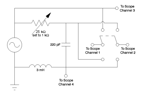
A potentiometer, a capacitor, an inductor and a signal generator are connected in series. On the oscilloscope you can read the voltage across the signal generator, the inductor and either the capacitor or the resistor (connected to the oscilloscope by the double-pole, double-throw switch at right in the photograph). When the generator produces a sine wave, you can see the phase relations of the voltages across the components, with respect to each other and to the voltage applied to the circuit. When you turn the dial of the signal generator through the resonant frequency (in either direction), all the voltages (except that across the signal generator, of course) increase to a maximum, then decrease thereafter. The phase relations also change as shown below. In addition, you can explore the effect of damping on the “quality,” or “Q,” of the circuit by adjusting the potentiometer (vide infra). Important note: The potentiometer in this circuit is large enough that you can take the system to critical damping, and then you can overdamp it. (See demonstration 72.66 -- Decaying oscillations in an LRC circuit.) Under these conditions the resonance becomes broad, and the change in frequency necessary to make either the capacitive reactance or the inductive reactance significantly greater than the resistance, is larger than for the underdamped situation. Also, the current maximum, and thus the voltage across each of the components, becomes smaller (vide infra).
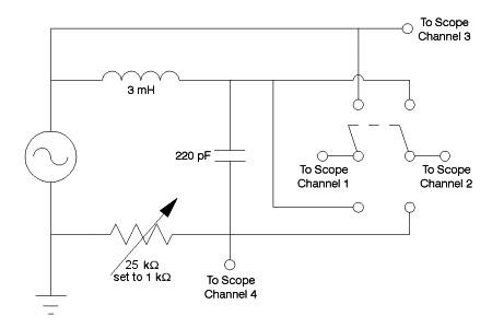
The schematic above shows the circuit (circuit B). A .pdf version of this schematic is available here to download and show on the data projector. Channel three on the oscilloscope shows the voltage applied by the signal generator to the circuit, and channel four shows the voltage across the inductor. Channels one and two are connected via a double-pole, double-throw switch to the ends of either the capacitor (switch down) or the resistor (switch up). The oscilloscope subtracts the signal on channel two from that on channel one, and displays the difference on a separate trace. This allows you to show the voltages across the capacitor and the inductor simultaneously, and to switch between the capacitor and the resistor.
The original circuit, which is still available, had the resistor and the inductor in the opposite positions, with oscilloscope channel four showing the voltage across the resistor, and the switch connected to the capacitor and the inductor, so that you could display the voltage across the resistor simulataneously with that across either the inductor or the capacitor (circuit A):
An overhead transparency of this circuit is also available, or you can download the .pdf file here. Traces obtained with both circuits appear below.
Please note: because of the phase relationships of the voltages across the three components, circuit B offers some advantage over circuit A. For this reason it is now the default. Either circuit allows you to illustrate in detail the behavior of an LRC circuit, however, and depending on which particular things you would like to be able to show simultaneously, you may prefer circuit A. If you do prefer circuit A, please state this when you request this demonstration.
The potential across the circuit, provided by the function generator, is E = Ep sin ωt, and the current is i = ip sin (ωt + φ), where the subscript “p” stands for “peak,” and φ is a phase factor. Since all the components are in series, the total potential across the circuit equals the sum of the potentials across the individual components, or E = VR + VC + VL. Now we must find the potential difference across each component, and the current in the circuit.
Perhaps the simplest way to do this is to take each component in turn, treating it as if it were the only component in the circuit. Starting with the resistor, we have VR = Ep sin ωt, which also equals iRR. Combining these gives us iR = (Ep/R) sin ωt. This tells us that the voltage and current in the resistor vary in phase with each other.
For the capacitor, we have VC = Ep sin ωt, and by the definition for capacitance, VC = q/C. Together, these give q = EpC sin ωt. Since current, iC = dq/dt, the current in the capacitor is iC = ωCEp cos ωt. This indicates that the voltage and current are out of phase with each other by 90°, or one quarter cycle, and that the voltage, which starts at zero when the current is at its maximum, lags the current. If we set φ = -90° in the equation for current in the first paragraph above, and then use the addition formula for sines, we get i = ip cos ωt. To make this similar to the equation for the resistor, we can write it as iC = (Ep/XC) cos ωt, where XC = 1/ωC. XC is the capacitive reactance. It is analogous to resistance, and its units are ohms. We can see from the equations above that the maximum voltage across the capacitor is VC, p = ipXC.
For the inductor, we have VL = Ep sin ωt, and by the definition for inductance, VL = L(di/dt). Together, these give di = (Ep/L) sin ωt dt. So the current, iL, is the integral of this, or iL = -(Ep/ωL) cos ωt. The voltage and current are again out of phase by 90°, or one quarter cycle. This time, when the voltage starts at zero, the current is negative and reaches its maximum one quarter cycle after the voltage has reached its maximum. So the voltage leads the current, and the phase factor is +90°. Putting this into the first equation gives us i = -ip cos ωt. As we did for the capacitor, we can cast this equation as iL = -(Ep/XL) cos ωt, where XL = ωL. XL is the inductive reactance. It is also analogous to resistance, and its units are also ohms. We also see from the equations that the maximum voltage across the inductor is VL, p = ipXL.
Now we must find the current in the whole circuit. We know that the voltages must add according to E = VR + VC + VL. Since these voltages all vary with time and have different phases with respect to each other, we cannot simply add the maximum voltages for which we derived expressions above, then divide to obtain the current. One way to deal with this is to represent each voltage/current pair (i.e., V and i for each component) as a pair of phasors, that is, vectors that rotate counterclockwise with angular frequency ω, whose magnitudes are the peak values of the voltage and current, and whose projections on the y-axis give the instantaneous values of voltage and current. The algebraic sum of these instantaneous projections gives E. Their vector sum gives Ep. VC and VL are 180° apart, and both are 90° to VR. Therefore, we can obtain Ep by Ep = √(VR2 + (VL - VC)2), where all the voltages are the peak voltages. This equals √((ipR)2 + (ipXL - ipXC)2), and we obtain Ep = ip√(R2 + (XL - XC)2). The quantity that contains the resistance, inductive reactance and capacitive reactance is the impedance, usually denoted Z, and ip = Ep/Z. If we substitute the expressions for the inductive and capacitive reactances and rearrange, we obtain ip = Ep/√(R2 + (ωL - 1/ωC)2).
From the relationships among the phasors, we obtain the phase angle, φ, for the current in the circuit, from tan φ = (VL - VC)/VR, where, again, all voltages are peak voltages. This equals i(XL - XC)/iR = (XL - XC)/R.
Now we notice something interesting about the expression for the current in the LRC circuit, which is that the current has a maximum when the inductive reactance equals the capacitive reactance, or ωL = 1/ωC. At this point the inductive and capacitive terms in the expression for Z cancel, and the impedance becomes purely resistive. This condition, where the current is a maximum, is called resonance. By rearranging the preceding equality, we find that it obtains when ω = 1/√LC. For our circuit, L = 3 mH, C = 220 pF, and 1/√LC = 1.2 × 10⁶ rad/s, or, dividing by 2π, 200 kHz. At this point, the expression above for maximum current becomes ip = Ep/R, or, generally, i = Ep sin ωt/R. Note that at resonance, since XL = XC, the phase angle for the current is zero.
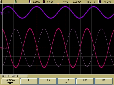
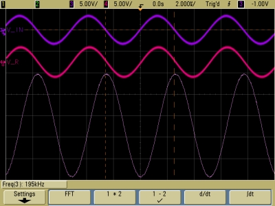
Now, at long last, we get to the oscilloscope traces that illustrate the workings of this circuit. Below are two oscilloscope displays taken at resonance. The top trace (blue) is the voltage applied by the function generator. The bottom traces are VL (pink) and either VC or VR (light purple). The frequency at resonance is 195 kHz, close to that calculated above from the nominal component values.
For all of the traces shown below, the variable resistor was set to 1 kΩ.
Note that VC and VL are approximately three times greater than E, and that VR and E are equal. (The vertical scale for all three traces in each panel is 5.00 V/div.) By far the greatest potentials appear across the capacitor and the inductor, but they are equal and 180° out of phase with each other, so they add to zero, and the potential across the resistor equals the applied potential. Thus, all the potentials around the circuit add to equal the applied potential.
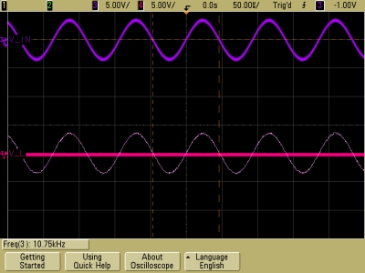
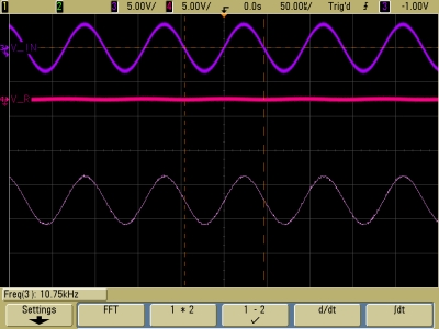
If we lower the frequency below the resonant frequency, XC (= 1/ωC) increases and XL (= ωL) decreases. If we lower the frequency far enough, XC becomes much larger than XL, and the contribution from the LC part of the circuit becomes mostly capacitive. At 10.75 kHz, XC equals approximately 67 kΩ, and XL is about 200 Ω. Together, these are much greater than the 1-kΩ resistance of the variable resistor (√(XC2 - XL2) ≈ 67 kΩ). So most of the applied voltage appears across the capacitor:
The voltage across the capacitor is now roughly equal to the applied voltage, and it is in phase with it. Since XL < XC, the phase angle for the current in the circuit is negative.
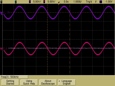
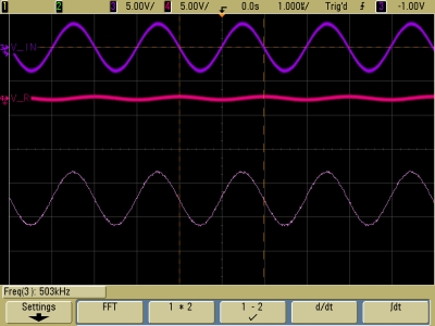
If we increase the frequency above the resonant frequency, XL (= ωL) increases and XC (= 1/ωC) decreases. At 503 kHz, XL is about 9.48 kΩ, and XC is about 1.44 kΩ. The impedance of both together is about 9.37 kΩ (√(XL2 - XC2) ≈ 9.37 kΩ). So most of the applied voltage appears across the inductor:
Now the voltage across the inductor is essentially in phase with, and roughly equal to, the applied voltage. Since XL > XC, the phase angle for the current in the circuit is positive.
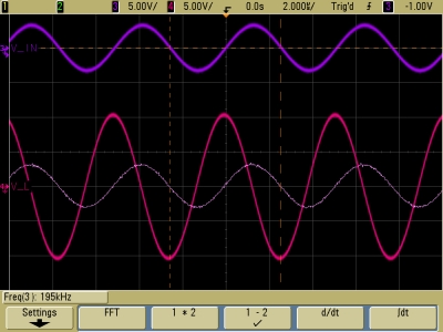
As noted above, if you wish to show the voltages across the resistor and either the capacitor or the inductor at the same time, it is possible to arrange this demonstration to do so. Below are the traces that you obtain this way.
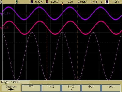
First, at resonance:
Again, VR and E are equal, and VC and VL are approximately three times greater. By far the greatest potentials appear across the capacitor and the inductor, but they are equal and 180° out of phase with each other, so they add to zero, and the potential across the resistor equals the applied potential. Thus, all the potentials around the circuit add to equal the applied potential.
Now below resonance:
Now above resonance:
An important property of LRC circuits is the “quality,” or “Q.” As the oscilloscope traces above show, if we were to plot the rms current in the LRC circuit vs. the frequency of the applied potential, we would obtain a curve that had a symmetrical peak centered at the resonant frequency of the circuit. The greater the resistance, R, the lower the peak maximum and the broader the peak. Conversely, for smaller resistance, the maximum increases and the peak becomes narrower. One usually characterizes this curve by its full width at half maximum, or half width, Δω/ω. One can show that this is approximately equal to √3R/ωL. Q is ωL/R, so that Δω/ω ≈ √3/Q. By adjusting the variable resistor and then sweeping the frequency, you can show how the current maximum and peak width change with R.
References:
1) Halliday, David and Resnick, Robert. Physics, Part Two, Third Edition (New York: John Wiley and Sons, 1977), pp. 856, 858-863, 866-868, 878.